The global IC Packaging Solder Ball market was valued at US$ 251 million in 2024 and is anticipated to reach US$ 388 million by 2031, witnessing a CAGR of 6.5% during the forecast period 2025-2031.
The IC Packaging Solder Ball Market is gaining strong traction as semiconductor packaging technologies evolve to meet the performance demands of next-generation electronics. Solder balls—tiny metallic spheres used to connect semiconductor packages to printed circuit boards (PCBs)—play a critical role in ensuring electrical conductivity, mechanical stability, and thermal management. With the rise of miniaturized, high-performance integrated circuits, demand for advanced solder ball materials and precise manufacturing processes continues to grow worldwide.
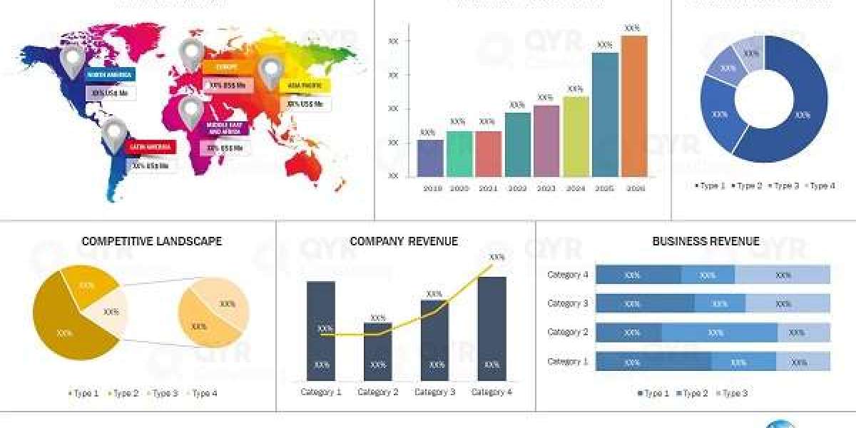
Read Full Research Report: https://www.qyresearch.in/report-details/1087346/Global-IC-Packaging-Solder-Ball-Market-Insights
Market Overview
IC packaging solder balls are primarily used in Ball Grid Array (BGA), Chip-Scale Package (CSP), and Flip-Chip designs, forming essential interconnects between the semiconductor die and the substrate. These solder balls provide low-resistance electrical paths while absorbing mechanical stress during thermal cycling. The increasing adoption of advanced packaging technologies in smartphones, automotive electronics, data centers, and artificial intelligence (AI) hardware is fueling market expansion.
The global IC Packaging Solder Ball Market is expected to witness steady growth over the next decade, supported by trends such as miniaturization of devices, rising complexity of integrated circuits, and the transition toward lead-free and environmentally sustainable solder materials.
Key Market Drivers
1. Growth in Semiconductor Manufacturing
The ongoing boom in global semiconductor production is a primary growth driver for the IC packaging solder ball market. As fabrication facilities ramp up production of logic chips, memory devices, and power semiconductors, the demand for high-reliability packaging materials increases. Solder balls ensure stable connections in high-density integrated circuits, making them vital components in modern chip packaging.
2. Rising Adoption of Advanced Packaging Technologies
The semiconductor industry is transitioning from traditional wire-bond packaging to advanced methods such as Flip-Chip Ball Grid Array (FCBGA) and Wafer-Level Chip-Scale Packaging (WLCSP). These designs require precisely engineered solder balls with uniform size distribution, strong adhesion, and high melting stability. The push for higher I/O counts, lower parasitic inductance, and improved heat dissipation continues to drive technological innovation in solder ball production.
3. Increasing Demand for Consumer and Automotive Electronics
The proliferation of consumer electronics—smartphones, tablets, wearables, and gaming consoles—has significantly boosted solder ball consumption. In the automotive sector, the rapid adoption of electric vehicles (EVs) and advanced driver assistance systems (ADAS) has created a need for durable solder materials that can withstand high thermal and mechanical stress. This expansion into automotive and industrial electronics is broadening the market’s application base.
4. Shift Toward Lead-Free and Eco-Friendly Alloys
Environmental regulations and sustainability goals are pushing the semiconductor packaging industry to transition from lead-based to lead-free solder compositions. Modern solder balls are now made from tin-based alloys (such as Sn-Ag-Cu) that offer superior reliability, corrosion resistance, and thermal fatigue performance. This trend aligns with global initiatives to reduce hazardous materials in electronic manufacturing.
Market Trends
- Miniaturization and Fine-Pitch Interconnects: As chip architectures shrink, manufacturers are developing smaller-diameter solder balls that enable finer pitch interconnections without compromising strength or conductivity.
- Enhanced Material Formulations: Advances in alloy composition, flux chemistry, and surface coatings are improving solder wetting behavior and joint reliability under high-temperature operation.
- Automation and Precision Manufacturing: The use of automated ball-placement equipment and optical inspection systems ensures consistent quality and alignment accuracy during packaging.
- Integration with 3D Packaging and System-in-Package (SiP): Emerging 3D stacking technologies require advanced solder materials capable of handling multiple interconnection layers while maintaining signal integrity.
Regional Insights
The Asia-Pacific region dominates the IC Packaging Solder Ball Market, driven by its strong semiconductor manufacturing ecosystem, particularly in countries leading global chip fabrication and assembly. North America and Europe are also key markets, supported by technological innovation and growing investments in local semiconductor supply chains. Meanwhile, emerging economies are expanding their packaging and testing capacities, further contributing to regional market diversification.
Future Outlook
The future of the IC Packaging Solder Ball Market is closely tied to innovations in semiconductor packaging, miniaturization, and material engineering. As the electronics industry moves toward heterogeneous integration and chiplet-based architectures, demand for high-precision solder materials will continue to rise. Manufacturers are expected to focus on developing advanced lead-free alloys, improved thermal cycling performance, and compatibility with next-generation substrates.
In conclusion, the IC Packaging Solder Ball Market is poised for sustained growth, fueled by global semiconductor advancements, the adoption of eco-friendly materials, and the relentless pursuit of higher performance and reliability. As packaging technologies evolve, solder balls will remain a vital enabler of connectivity, durability, and efficiency in the rapidly transforming electronics landscape.
QY Research established in 2007, focus on custom research, management consulting, IPO consulting, industry chain research, data base and seminar services. The company owned a large basic data base (such as National Bureau of statistics database, Customs import and export database, Industry Association Database etc), expert’s resources (included energy automotive chemical medical ICT consumer goods etc.
Contact Us:
QY Research, INC.
315 Work Avenue, Raheja Woods,
Survey No. 222/1, Plot No. 25, 6th Floor,
Kayani Nagar, Yervada, Pune 411006, Maharashtra
Tel: +91-8669986909
Emails - [email protected]


