The global Wafer CMP Equipment market was valued at US$ million in 2024 and is anticipated to reach US$ million by 2031, witnessing a CAGR of %during the forecast period 2025-2031.
The Wafer CMP (Chemical Mechanical Planarization) equipment market is expanding steadily as chipmakers push toward advanced nodes, 3D structures, and heterogeneous integration. CMP remains a mission-critical step that ensures global and local planarization before lithography, enabling tighter line widths, improved pattern fidelity, and higher yields. As logic and memory manufacturers accelerate ramps at sub-5nm, Gate-All-Around (GAA) nodes, advanced DRAM, and high-layer 3D NAND, demand for high-throughput, low-defect CMP tools with superior process control is rising. In parallel, specialty technologies—SiC and GaN power devices, MEMS, sensors, and compound semiconductors—are broadening CMP use cases and driving tool customization.
Read Full Research Report: https://www.qyresearch.in/report-details/4560193/Global-Wafer-CMP-Equipment-Market-Insights
Market Drivers
Key growth drivers include relentless device miniaturization, more metal layers per stack, and complex integration schemes that multiply CMP steps per wafer. Foundry/logic customers require exceptional within-wafer and wafer-to-wafer uniformity to protect yield at cutting-edge nodes, while memory makers seek cost-per-bit reductions through higher vertical stacking—both trends lift CMP intensity. Capacity additions across Asia-Pacific and renewed fab investments in North America and Europe further underpin tool orders. The shift toward wide bandgap power semiconductors also stimulates demand for CMP equipment capable of handling hard materials with tight total thickness variation (TTV) targets.
Technology Landscape
Modern CMP platforms integrate precise carrier pressure control, multi-zone polishing heads, optimized pad/conditioning strategies, and endpoint metrology (optical, motor-current, friction, and acoustic signatures). Advanced systems pair real-time sensors with closed-loop algorithms to maintain removal rates and uniformity across consumable drift. Post-CMP clean modules mitigate micro-scratches, metallic residues, and defectivity. Automation—robotic wafer handling, fault detection and classification, and predictive maintenance—raises uptime and reduces cost of ownership. On challenging materials like SiC, sapphire, or III-V compounds, next-generation slurries and pads combined with ultra-stable platen dynamics deliver improved planarity at lower defect densities.
Notable Trends
Three trends stand out. First, more in-situ metrology: integrated film thickness and defect monitoring shorten feedback cycles and enable adaptive recipes. Second, sustainability: fabs are targeting lower slurry consumption, water recycling, and longer pad life; CMP tools with efficient slurry distribution, reclaim loops, and smart conditioning directly support ESG goals. Third, digitalization: equipment vendors are embedding analytics, digital twins, and AI-assisted tuning to accelerate process setup, reduce variability, and predict consumable change points—vital for high-mix, high-volume environments.
Market Segmentation
By device type, demand splits across logic/foundry, memory (DRAM and 3D NAND), and power/analog/compound semiconductors. By application, key CMP steps include oxide ILD, tungsten, copper/low-k, STI, poly/fin/gate, and emerging interposer/wafer-level packaging processes. Tool classes range from high-throughput 300 mm platforms for leading-edge fabs to flexible 200 mm systems serving specialty and legacy nodes. Service and software—process optimization, health monitoring, and factory integration—are growing revenue streams alongside hardware and consumables.
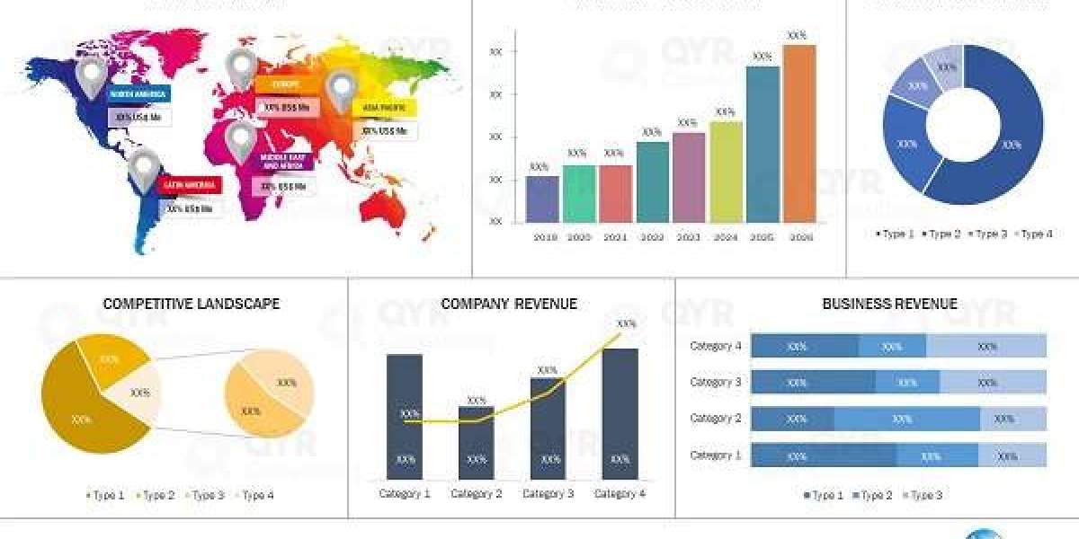
Regional Insights
Asia-Pacific leads installed base and new tool purchases, anchored by major foundries and memory producers in Taiwan, South Korea, China, and Japan. North America benefits from onshoring incentives and advanced logic investments, while Europe’s growth is supported by analog, power, and automotive semiconductor capacity. Across all regions, greenfield megafabs and brownfield expansions require CMP fleets that scale throughput without sacrificing defectivity control.
Competitive Landscape
The competitive field includes global wafer fab equipment leaders and specialized CMP providers offering end-to-end solutions: polishers, conditioners, post-CMP cleaners, and integrated metrology. Differentiation hinges on removal-rate stability, planarity at advanced topographies, particle control, cost-of-ownership, and the strength of applications support. Strategic collaborations with slurry and pad suppliers, along with joint development programs at customer fabs, are common paths to faster recipe maturity.
Outlook
With more CMP steps per wafer, tougher materials, and stricter uniformity specs, the wafer CMP equipment market is poised for sustained growth. Vendors that deliver data-driven process control, lower chemical and water usage, and rapid time-to-recipe will capture outsized share. As AI/ML-enabled tuning, advanced metrology, and sustainability features become standard, CMP will remain a cornerstone of yield and performance at the leading edge—while simultaneously unlocking quality and cost advantages for specialty and legacy nodes.Top of Form
Bottom of Form
QY Research established in 2007, focus on custom research, management consulting, IPO consulting, industry chain research, data base and seminar services. The company owned a large basic data base (such as National Bureau of statistics database, Customs import and export database, Industry Association Database etc), expert’s resources (included energy automotive chemical medical ICT consumer goods etc.
Contact Us:
QY Research, INC.
315 Work Avenue, Raheja Woods,
Survey No. 222/1, Plot No. 25, 6th Floor,
Kayani Nagar, Yervada, Pune 411006, Maharashtra
Tel: +91-8669986909
Emails - [email protected]