The global Wafer Level Chip Scale Package (WLCSP) market was valued at US$ million in 2024 and is anticipated to reach US$ million by 2031, witnessing a CAGR of %during the forecast period 2025-2031.
The wafer level chip scale package (WLCSP) market is experiencing strong growth as consumer electronics, automotive, and industrial applications increasingly adopt miniaturized, high-performance semiconductor packaging solutions. WLCSP is one of the most advanced packaging technologies, offering benefits such as reduced size, enhanced performance, and lower production costs. With growing demand for smartphones, IoT devices, and automotive electronics, the global WLCSP market is set to expand at a significant pace.
Read Full Research Report: https://www.qyresearch.in/report-details/5936087/Global-Wafer-Level-Chip-Scale-Package-(WLCSP)-Market-Insights
What is Wafer Level Chip Scale Package (WLCSP)?
WLCSP is a semiconductor packaging technology in which integrated circuits (ICs) are packaged directly at the wafer level rather than after the wafer is diced into individual chips. This process allows manufacturers to produce extremely compact and high-density packages.
Key advantages include:
- Ultra-compact size and reduced footprint
- Enhanced electrical performance with shorter interconnects
- Cost-effectiveness through wafer-level batch processing
- Improved thermal performance and reliability
WLCSP is widely adopted in mobile, wearable, and high-speed computing devices due to its miniaturization benefits.
Market Drivers
Growing Smartphone and Consumer Electronics Demand
Smartphones, tablets, and wearables dominate WLCSP applications. With increasing need for compact, lightweight, and high-performance devices, WLCSP adoption is accelerating.
Rising Internet of Things (IoT) Applications
IoT-enabled sensors, smart home devices, and industrial IoT equipment require compact semiconductor packaging. WLCSP provides the performance and form factor needed for these applications.
Automotive Electronics Expansion
Advanced driver assistance systems (ADAS), infotainment, and electric vehicle (EV) systems are driving demand for WLCSP in the automotive sector.
Cost Efficiency and Performance Improvements
WLCSP offers reduced interconnect delays, higher bandwidth, and better heat dissipation compared to traditional packaging, making it highly attractive to semiconductor manufacturers.
Market Segmentation
The WLCSP market can be segmented by:
- Type: Fan-in WLCSP, fan-out WLCSP
- Application: Consumer electronics, automotive, industrial, healthcare, telecommunications
- End User: Semiconductor manufacturers, electronics OEMs, automotive companies, IoT device makers
Fan-in WLCSP dominates in consumer electronics, while fan-out WLCSP is gaining traction in applications requiring more I/O density and reliability, such as automotive and high-performance computing.
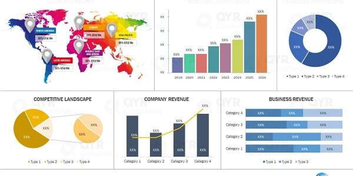
Regional Insights
- Asia-Pacific leads the market, with China, Taiwan, South Korea, and Japan being global hubs for semiconductor manufacturing and consumer electronics production.
- North America shows strong growth, driven by innovation in IoT, automotive electronics, and semiconductor R&D, particularly in the U.S.
- Europe follows, supported by automotive and industrial applications in Germany, France, and the UK.
- Latin America is emerging, with Brazil and Mexico expanding electronics and telecom infrastructure.
- Middle East & Africa show gradual adoption, supported by rising demand for consumer electronics and digital transformation initiatives.
Competitive Landscape
The WLCSP market is competitive, with leading semiconductor manufacturers and packaging companies focusing on miniaturization, performance enhancement, and cost reduction. Key players include:
- Taiwan Semiconductor Manufacturing Company (TSMC)
- ASE Group
- Amkor Technology, Inc.
- STATS ChipPAC Ltd.
- Jiangsu Changjiang Electronics Technology (JCET)
- Texas Instruments Incorporated
- Fujitsu Semiconductor Limited
These companies are investing in advanced fan-out WLCSP, 3D packaging, and next-generation semiconductor technologies to meet evolving industry needs.
Challenges and Opportunities Challenges:
- Technical limitations in handling very large chips
- High initial investment in advanced packaging facilities
- Reliability concerns in extreme operating environments
Opportunities:
- Expansion in wearable devices and smart healthcare technologies
- Rising adoption in electric vehicles and ADAS systems
- Growing demand for 5G-enabled devices and high-speed computing
- Development of fan-out WLCSP for higher I/O applications
Future Outlook
The wafer level chip scale package market is set to grow significantly as industries continue to demand smaller, faster, and more energy-efficient devices. Future trends will include:
- Wider adoption of fan-out WLCSP in automotive and industrial applications
- Integration with 3D IC and system-in-package (SiP) technologies
- Miniaturized packaging solutions for medical implants and wearable healthcare devices
- Rising demand for semiconductor packaging in AI, cloud computing, and 5G infrastructure
As the global semiconductor industry moves toward advanced packaging technologies, WLCSP will remain a critical solution for enabling compact, high-performance, and cost-effective devices.
QY Research established in 2007, focus on custom research, management consulting, IPO consulting, industry chain research, data base and seminar services. The company owned a large basic data base (such as National Bureau of statistics database, Customs import and export database, Industry Association Database etc), expert’s resources (included energy automotive chemical medical ICT consumer goods etc.
Contact Us:
QY Research, INC.
315 Work Avenue, Raheja Woods,
Survey No. 222/1, Plot No. 25, 6th Floor,
Kayani Nagar, Yervada, Pune 411006, Maharashtra
Tel: +91-8669986909
Emails - [email protected]
Web - https://www.qyresearch.in